

Taiwan Semiconductor Manufacturing Company (better known as TSMC) is preparing to launch mass production of its processors with a 2-nanometer lithography process (N2).
Expectations are sky-high and early data suggest a commercial success that could eclipse any previous technological generation.
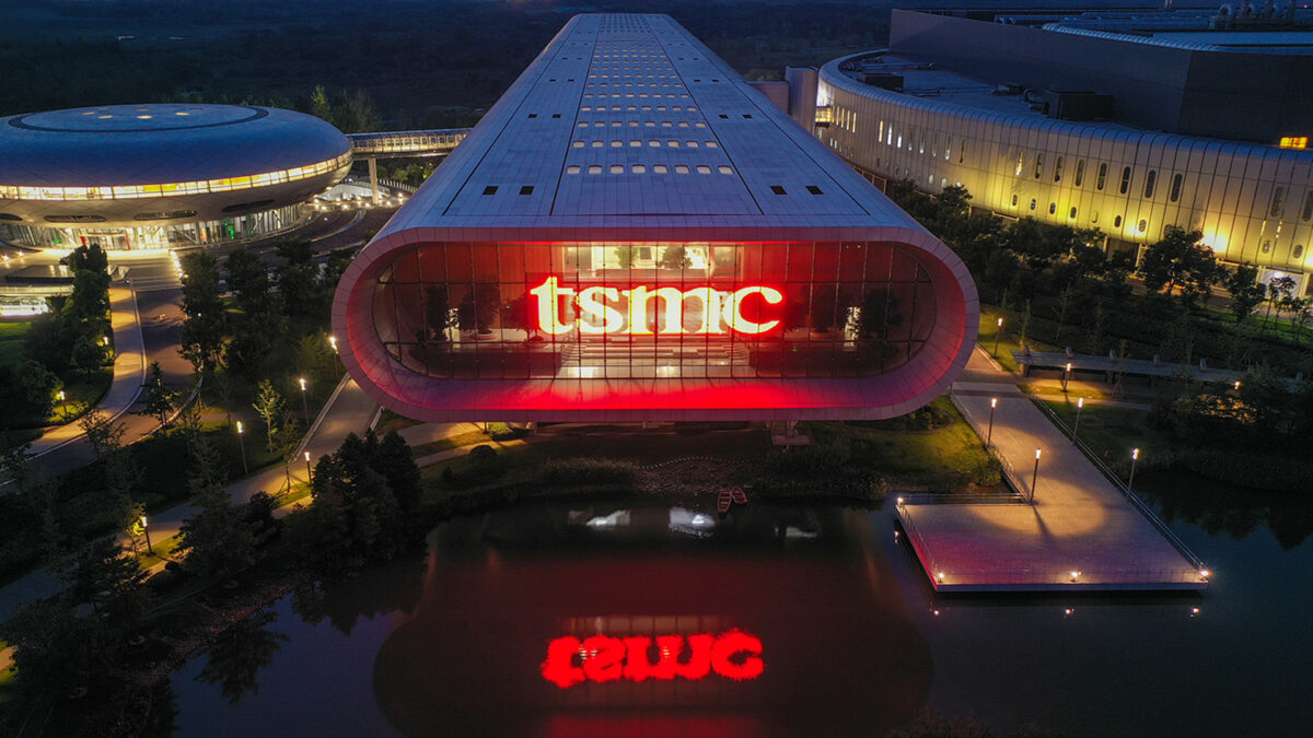
TSMC prepares for an unprecedented 2 nm chip production
According to the latest industry leaks, the number of tape-outs, i.e., the final design phase of a chip before it goes into production, for the 2 nm technology is one and a half times that recorded for the 3 nm generation.
This 50% increase in tape-out-ready designs testifies to a hunger for performance and energy efficiency that has no equal in silicon’s recent history.
The Unrivaled Dominance in AI
The driving force behind this frenzy is, unsurprisingly, the aggressive expansion of the artificial intelligence sector.
New details from sources close to the supply chain indicate that TSMC is set to maintain an unassailable 95% market share in the AI accelerators sector. This de facto monopoly on cutting-edge technology will allow the company to reach new revenue heights.
Production forecasts are equally astonishing: by the end of 2026, the monthly production target for wafers based on this lithography is expected to reach the colossal figure of 140,000 units.
Even Intel, which is trying to revive its foundries with the 18A technology for Panther Lake processors, seems intent on exploring TSMC’s N2 process for several of its products, confirming the current technological supremacy of the Taiwanese giant.
Financial outlook and rapid market adoption
The adoption of the 2 nm technology is happening at a pace that is rewriting the company’s financial guidance.
It is estimated that, by Q3 2026, revenues generated by the 2 nm processes alone will exceed the combined revenue of 3 nm and 5 nm technologies. This figure serves as a key indicator of how quickly the industry is migrating to the new lithography, abandoning the previous generations much faster than in past cycles.
This acceleration is largely due to the competition among tech giants consumer. Apple, confirming itself as TSMC’s most important customer also in 2024, would have already secured over half of the initial 2 nm production capacity. Most of these wafers will be destined for the upcoming A20 and A20 Pro chips, which will power the iPhone 18 series, followed by the M6 chip planned for OLED MacBook Pros.
Rivals’ Strategy and the Evolution of N2P
With Apple having monopolized the initial capacity, the question naturally arises how the historical rivals such as Qualcomm and MediaTek will respond. MediaTek has already announced the tape-out of its first SoC on this lithography, and rumors suggest that all three major players will announce their 2 nm SoCs in the same month.
To circumvent the initial production capacity saturation absorbed by Cupertino, TSMC appears to have a ready solution: an improved iteration of the node, named N2P.
Although it offers incremental improvements, the N2P node could prove to be strategic for Apple’s competitors. This variant would allow Qualcomm and MediaTek to target higher CPU clock frequencies, while ensuring adequate shipment volumes to satisfy their customers without waiting for the base N2 node capacity to free up.
Finally, despite TSMC’s technological lead, there are rumors reported by Morgan Stanley that Apple is still evaluating the use of Intel Foundry Services (IFS) for its M-series chips.
However, this interest is believed to be limited to budget models for affordable Macs. Given TSMC’s historical reliability and its exclusive access to the most advanced nodes, it seems unlikely that another foundry could threaten its leadership for several years to come.

