

The microprocessor industry never slows down. While the market awaits the arrival of the first Apple chipsets built with a 2 nm process, expected for the upcoming iPhone 18 lineup featuring SoCs A20 and A20 Pro, the focus of manufacturers is already projected toward the next step.
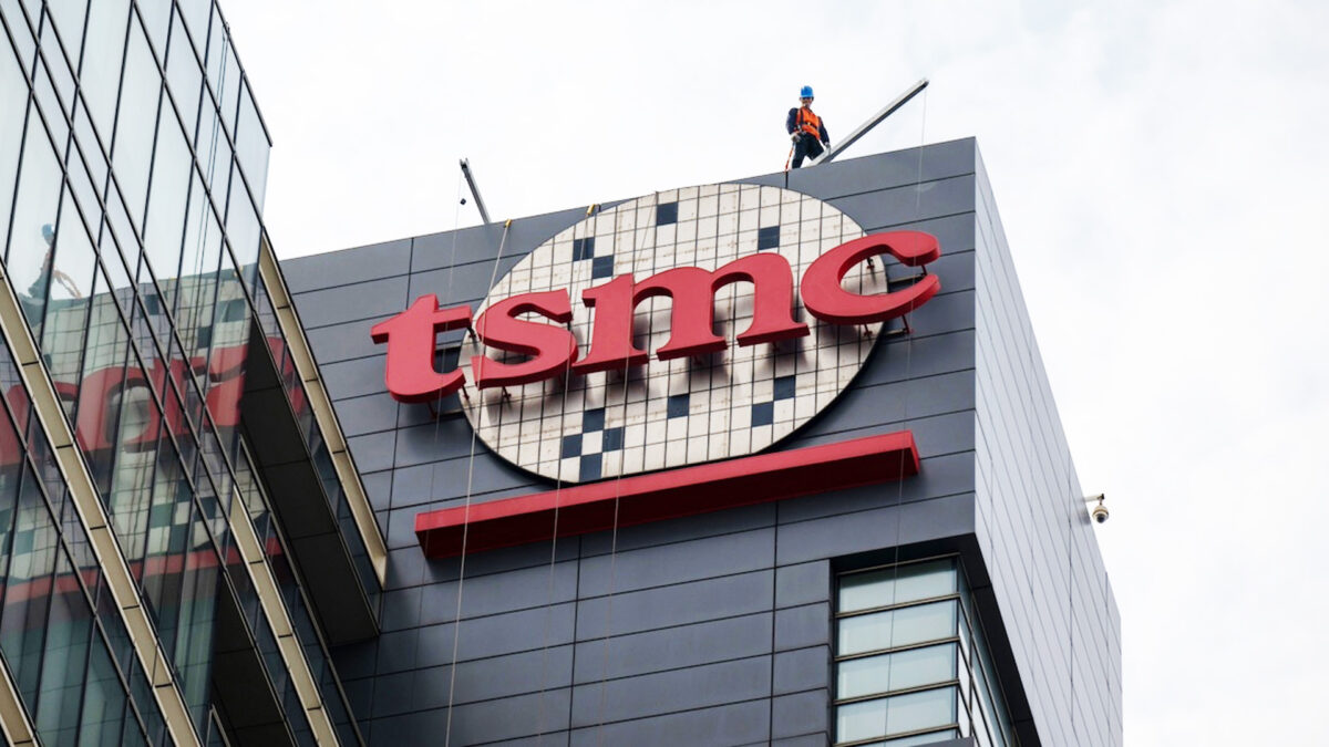
The exclusive partner of the Californian company for semiconductor supply, TSMC, is laying out an extremely ambitious roadmap for the coming years.
According to recent industry reports, the chip giant is planning to surpass a formidable technical milestone: to go below the single nanometer threshold, initiating prototype production of these new components by 2029.
TSMC sub-nanometer: milestones on the path to extreme miniaturization
Before reaching this frontier, TSMC will have to complete several intermediate stages of great significance. Currently, the company is struggling to keep up with the enormous demand for the 2 nm architecture, but mid-term plans are already consolidated.
By 2028, the Taiwanese manufacturer expects to start mass production of the 1.4 nm process, formally identified with the designation A14.
This generation promises improvements of up to 30% in terms of absolute computing performance as well as the fundamental energy efficiency. At the same time, the company is gearing up to fulfill orders for the A16 node, based on a 1.6 nm architecture, another step for customers needing top-tier compute power in the market.
However, the real test will be the transition to sub-nanometer processes. Although the emerging documentation does not explicitly indicate the final customers for this ultra-advanced technology, it is highly likely that Apple will be among the first adopters, thanks to its long-standing prior arrangement.
To support such an effort, TSMC is mobilizing enormous structural and logistical resources. The operations will specifically involve the stabilimento A10 located in Tainan, supported by the capabilities of the impianti P1-P4.
The initial target set by management envisions a productive capacity of 5.000 wafer al mese during the testing phase. This is a volume calculated to calibrate the new lithographies, optimize machinery with microscopic precision, and evaluate the stability of the entire assembly line.
Market impact and production hurdles
Current pressure on foundries is driven not only by the normal demands of the smartphone sector, but also by the overwhelming and sudden need for hardware accelerators for artificial intelligence.
The global demand for iPhone remains consistently high, and it would not be surprising at all to see Apple willing to pay a substantial premium to secure exclusive lots of the first sub-nanometer chips, replicating strategies already adopted in previous years.
Although the prospects are promising, the path to mass production at such scales is full of practical difficulties. Yield, i.e., the percentage of defect-free chips per wafer produced, represents the main obstacle.
Precisely because of the extreme complexity in obtaining minimal waste at these sizes, there are growing rumors that several smartphone manufacturers could be soon forced to recalibrate their commercial offers.
In the absence of adequate supply volumes or due to prohibitive costs, the latest-generation processors would be reserved exclusively for Ultra-tier devices, further widening the performance fragmentation within the same premium product lines.

